![]()
작성일: 2004.02.23
TechXclusives...
By Peter Alfke Director, Applications Engineering, Xilinx San Jose
- Publication Data: 04/02/2003 -
Most FPGA designs are purely digital, and are usually also synchronous. Occasionally, however, there is a need for special asynchronous circuitry: a push-button debouncer, input Schmitt trigger, low-frequency oscillator, frequency doubler, output-voltage booster, or truly asynchronous clock multiplexer. These seemingly trivial circuits can lead to an inordinate amount of trouble if implemented improperly. Here are six proven designs that might come in handy in special situations.
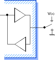
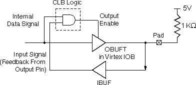
Interfacing a switch to fast CMOS logic is not trivial. Any mechanical switch bounces when it is being closed (and even when it opens). The bounce can last for milliseconds. The safest interface is from a double-throw switch into the Set and Reset of a CMOS latch. The circuit below uses feedback in the I/O as a latch, and thus requires only a single pin.
Configure the output with a low drive strength to minimize the short change-over current spike.
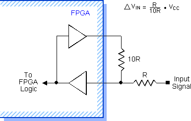
This circuit provides adjustable input hysteresis. The difference between upward-going and downward-going input threshold voltage is equal to the supply voltage multiplied by the ratio of the two resistors.
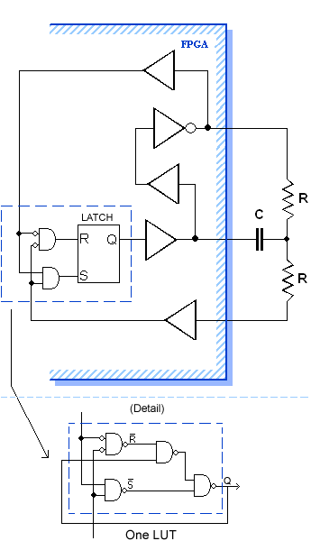
This RC oscillator is, to a first-order, insensitive to variations in Vcc, input threshold, and thus temperature. The oscillator starts and runs under any combination of external conditions -- it cannot stop. The internal latch prevents fast double-pulses while the input slowly passes through the input threshold. The only drawback is the need for three dedicated device pins.
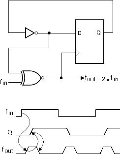
An input signal can be doubled in frequency, provided the resulting 2f clock can tolerate cycle-to-cycle jitter caused by an imperfect input duty cycle. The circuit below generates an output pulse in response to each transition of the input.
The output rising edge is delayed one TILO from either input transition. The output High time is the sum of a clock-to-Q delay plus two TILO delays, about 2 ns in a fast part. This output pulse clocks other flip-flops on the same die reliably. (At a low temperature and high VCC, the pulse will be shorter, but the flip-flop response is also faster under these conditions.)
Any control input that prevents the flip-flop from toggling changes the output frequency to fout = fin.
This asynchronous circuit is frowned upon by all true digital designers. It should only be used as a tool of last resort. Note that the DLL or DCM in all Virtex or Spartan-II devices provide frequency doubling for free, if the input frequency is larger than 25 MHz. The frequency-doubler circuit shown below has no minimum frequency limitation.
When a CMOS-level 5V input is driven, the output High voltage from a 3.3V device is marginal. If the 3.3V output is 5V tolerant, a pull-up resistor to 5V can pull the output that is in a 3-state condition all the way to 5V. The problem is the slow rise time of tens or hundreds of nanoseconds, which is caused by the capacitive load. This circuit greatly reduces the rise time by keeping the active pull-up engaged until the output voltage has passed the threshold voltage of ~1.6V. Slowing down the internal input signal and 2-input AND gate will speed up the rise time even more. (For more information, see this.)
This circuit can also be used to speed up the interface between 2.5V and 3.3V devices.
Asynchronously switching between two unrelated clock frequencies will produce runt pulses and glitches that make the system unreliable. The circuit shown below illustrates a solution to these problems.
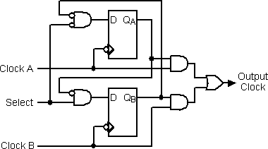
When the SELECT input is stable (either High or Low), the two control flip-flops are in opposite states, and one of the two clock inputs drives the clock output.
When the SELECT input changes, there is no immediate impact until after the next falling edge of the originally-selected clock source, which also resets its control flip-flop. The Output Clock signal will then stay Low beyond the next falling edge of the newly selected clock, which sets its control flip-flop, causing the newly selected clock to drive the Output Clock.
Any clock-switching starts when the originally selected clock goes Low, and the Output Clock then stays Low until the newly selected clock has first gone Low and then High again. There can never be a runt pulse or output glitch.
If the timing of the SELECT input causes a control flip-flop to go metastable, this has no impact since the Output Clock is driven Low by the input clock (irrespective of the control flip-flop). Metastability must resolve itself within the clock Low time. Modern flip-flops resolve metastability in less than 2 ns (see the "Metastability Delay and Mean Time Between Failure in Virtex-II Pro™ FFs" TechXclusive from October, 2002).
This circuit assumes rising-edge triggering, and it requires both clocks to be free-running.
<!-- Source URL: Click Here -->
(C) Copyright 1994-2003 Xilinx, Inc. All Rights Reserved
![]()
![]() Send to a colleague |
Send to a colleague | ![]() Print this document
Print this document