Many HDL Designers write RTL code at a much lower level of abstraction than is actually necessary to achieve the desired end. Typically, such designers come from a board design background. They tend to think in terms of flip-flops, shift-registers, counters, decoders and so forth. Their code is usually structured in line with this mindset. By this I mean that a design will usually comprise multiple small blocks (or worse, separate files), these being wired up individually to produce the finished system.
Whilst there is nothing intrinsically wrong with this methodology, it does rather miss the point of using a Hardware Description Language in the first place. Such a knife & fork approach is limited for a number of reasons:
- The ratio of boilerplate to functional code is high. Consequently, it is inefficient in terms of coding time.
- Code structured this way is inflexible. Changes to the design are time consuming to incorporate.
- Readability suffers. Code of this style is written in terms of the structure of the finished circuit. It can be quite difficult to determine what such a design actually does.
The purpose of this document is to suggest ways for the designer to train himself/herself to think at a higher level of design abstraction, thereby releasing the full potential of the Hardware Description Language.
Incidentally, this article is equally applicable to exponents of VHDL and Verilog. The document assumes that the reader is familiar with at least one of the languages.
Let’s define ourselves a two input AND gate using VHDL:
LIBRARY ieee;

USE ieee.std_logic_1164.all;

USE ieee.std_logic_arith.all;
ENTITY AND2 IS


    PORT(


        A : IN     std_logic;


        B : IN     std_logic;


        Z : OUT    std_logic


    );

END AND2 ;
ARCHITECTURE behavioural1 OF AND2 IS

BEGIN
process( A, B ) is

       begin


    if A='1' and B='1' then


Z <= '1';


    else


        Z <= '0';


    end if;
end process;
END behavioural1;Nothing wrong with that I hear you say and, indeed, that is the way many designers work. But we could equally code up the architecture like this:
ARCHITECTURE behavioural2 OF AND2 IS

BEGIN
process( A, B ) is

    begin

    Z <= '0';
if A='1' and B='1' then

Z <= '1';

    end if;
end process;
END behavioural2;Notice that a default assignment is used to specify the most common outcome, namely logic ‘0’. That outcome is overridden in the single condition that both inputs are at logic ‘1’. The second style is a known as sequential design. When the simulator runs this piece of code, if both inputs are at logic ‘1’, then the output, Z, will be assigned twice, firstly to ‘0’ (by dint of the default) and then to ‘1’. The first technique, by contrast, is a parallel technique. For all combinations of input, the output is only ever assigned once. The code relies on detecting the unusual case (both inputs at logic ‘1’) and assigning the output to logic ‘1’ by branching. In all other cases, the default (else) branch is executed.
At face value, either of these techniques have their merits. However, as designs become more complicated, the power of the sequential technique comes to the fore.
Now let's design ourselves a very simple UART circuit. The model has serial data input, serial data output and a simple eight bit read/write bus (via which a microprocessor would send and receive bytes of serial data). Transmission protocol is START BIT (logic '0'), EIGHT DATA BITS (lsb 1st), STOP BIT (logic '1'). The memory interface is synchronous with a memory-map comprising two addresses as shown in Table 1.
|
Mnemonic |
Address |
Rea/Write/Clear |
Data |
Comment |
|||||||
|
7 |
6 |
5 |
4 |
3 |
2 |
1 |
0 |
||||
|
Tx |
0 |
Write |
D7 |
D6 |
D5 |
D4 |
D3 |
D2 |
D1 |
D0 |
Transmit Data Register |
|
Rx |
0 |
Read |
D7 |
D6 |
D5 |
D4 |
D3 |
D2 |
D1 |
D0 |
Receive Data Register |
|
Status |
1 |
Read |
|
|
|
|
|
TxReady |
RxError |
RxReady |
Status Register |
Table 1 UART Memory Map
Let’s code it up in a typical, convoluted, parallel style using VHDL (DUFF.vhd). In terms of a block diagram, we have something like (Block Diagram of badly coded UART). Notice that the basic function of the module is fairly apparent from the diagram (though it is rarely drawn out like this in practice). On the other hand, it is not readily apparent how the code functions and, more importantly, whether it contains any errors.
Note also that this module has been deliberately coded rather badly to illustrate a number of other points (though it does work). In particular, a number of artifacts (described here) were introduced.
Lets now consider the same block diagram as notional single large registers and a single amorphous blob of combinatorial logic (Block Diagram of elegantly coded UART). Having done that, we can re-code the module thus (RTL.vhd). Note that the entire module is now coded up as a single clockedLogic process. Notice that the function of the module is no longer readily apparent from the block diagram. However, the RTL itself is considerably more obvious in its behaviour.
What we’ve just done is prove to ourselves that all synchronous designs can be thought of as two simple elements:
- The registers that hold its present state and
- The combinatorial logic that determines its next state.
Once one has made that simple mental leap, it becomes obvious that RTL is simply a means of expressing the relationship between where the circuit is now and where it should go next. For any given state, the associated next state is simply a function of the present state and the circuit's inputs. The transfer function is defined by the clockedLogic process.
The next state (of the entire circuit, not just any single register) may simply be determined by executing the VHDL within the clockedLogic process. Consequently, a truth table for the module can be produced simply by running through the code for every possible combination of inputs. That is basically what the synthesiser does, notwithstanding the need to identify counters, adders and the like (as clearly it would not be possible, nor practical to run through every combination of inputs in the case of large counters). Having realised that, there’s no need ever again to write code containing explicit flip-flops, ALUs, counters or whatever. They can simply be incorporated in-line as required. Furthermore, it becomes easy to combine functions with fewer and fewer intermediate registers. For example, in the improved implementation of the UART, the three status bits TxReady, RxError & RxReady do not exist as explicit flip-flops, they are merely functions of the two state registers TxState & RxState. It was also possible to dispense with the input and output shift registers, TxShiftReg and RxShiftReg, thereby reducing the flip-flop count still further (at the cost of a little combinatorial logic). This would have quite difficult to achieve using the conventional coding style. Such savings are particularly useful in the case of Standard Cell ASIC designs, less so with FPGAs (where the ratio of combinatorial logic to flip-flops is fixed).
The module has also been converted into Verilog (RTL.v) to illustrate that the techniques are equally applicable to either language.
Subsequent discussion will build on this basic sequential coding methodology. Incidentally, the improved UART worked first time whereas the original, low level, implementation required considerable de-bugging.
Verilog has two kinds of assignment that may be used within a sequential block of code, namely the blocking assignment ( = ) and the non-blocking assignment ( <= ). A variable (in the programming sense) is known as a reg. A reg may therefore be assigned like this: x = 1; or like this: x<=1.
The blocking assignment is analogous to a normal variable assignment in any programming language, for example C. An assignment to a reg made with a blocking assignment will happen immediately. Any subsequent code that makes use of the variable so assigned will always see the newly assigned value. By contrast, the non-blocking assignment has a characteristic that is unique to the group of languages known as Hardware Description Languages. By assigning a reg with a non-blocking assignment, the change on that reg is scheduled (by the simulator) to occur after the present value has been sampled by any other assignments that use the value of that reg to calculate their respective next state.
Confused? Consider the following segment of Verilog using blocking assignments:
z = 0;

x = 1;

y = 2;

z = x + y;

y = 3;

w = z + y;
After execution of this code, the value of z will be 3 and the value of w will by 6. Now, consider the following similar code segment using non-blocking assignments:
z = 0;

x = 1;

y = 2;

z <= x + y;

y <= 3;

w = z + y;
After execution of this code, the value of z will be 3 as before but the value of w will by 2. How? Because z is assigned to the sum of x and y with a non-blocking assignment. Y is similarly assigned the value 3. W is then assigned to the sum of z and y. But the new values of these two variables are scheduled to happen after any other assignments that occur during the same simulation cycle (which is always the case within any given block of procedural code). Therefore, when w is assigned the sum of z and y, the values used are the old values of z and y, namely 0 and 2. Understanding of this basic tenet is vital for anyone intending using Verilog of VHDL.
VHDL has a similar capability, though the coding idioms are somewhat different (see Table 3). The VHDL equivalent of the blocking assignment is the variable assignment. VHDL has two types of variables (in the programming sense), the variable itself and the signal. Variables are assigned thus: x:=1; whereas signals are assigned like this: x<=1.
To all intents and purposes, variable assignments may be thought of like blocking assignments and signal assignments like non-blocking assignments. It does mean that the code fragment above (where y is assigned using both types of assignment) is not possible in VHDL. However, such a style is not generally a good idea anyway. The methodology described within this document is applicable to both languages in that it makes use of the common ground between the two. The beauty of this approach is that switching between languages doesn't require the brain to be re-calibrated!
What, you might ask, is the point of this peculiar method of assigning values to variables? Well the answer is because it facilitates the easy modelling of synchronous digital circuits. Most digital designs are synchronous in nature. A description of what constitutes a synchronous circuit is outside the scope of this document. It is assumed that the reader is familiar with the concept. The coding techniques described in this document are, by and large, applicable to the design of synchronous circuits.
The principal characteristic of a synchronous circuit is that each flip-flop output, Q, is loaded with the data present on its D input at the time of the rising (or occasionally falling) edge of some common clock signal. That data will be a function of one or more other flip-flops within the design, all of which will be loaded on the same clock edge. After the clock edge, the data present on the input, Q, will inevitably change. However, by that time, the original value of Q has been safely stored. It can be seen that this behaviour is exactly analogous to the operation of the non-blocking assignment (or VHDL signal assignment) described in the previous sections.
Answer: to assign the outputs of any clocked process that is used synchronously within another clocked process. That's it. Any other usage is in fact redundant (and to my mind superfluous). In VHDL, it is in fact impossible not to do this because all communications between processes have to be by means of signals. This document contends that that is the only time that non-blocking (or VHDL signal) assignments should be used. Most designers make much more liberal use of the non-blocking assignment than strictly necessary. I would argue that this obfuscates the code in that the real usage is lost amongst the non-essential uses. The example UART design (RTL.vhd) shows how it is done. The output readData, for example, is generated thus.
The corollary of this rule is that, synchronous outputs aside, all other assignments should be non-blocking (Verilog) or use variables (VHDL). Again, the UART example shows this. It can be seen that the VHDL and Verilog versions of this design are exactly analogous. In fact, this style lends itself to being auto-translated between the two languages.
In general, I would advocate only using non-blocking assignments (VHDL signal assignments) when their special behaviour is actually required. This is at odds with conventional wisdom but in keeping with a minimalist approach whereby code that does nothing and behaviour that isn't required are avoided.
An argument often put forward against using variables (or blocking assignments in VerilogSpeak) is that it is not possible to determine whether a particular declaration will synthesise to a flip-flop or not. Sadly, many otherwise expert RTL designers do not know how to determine the answer to this question. It is not the case that signals produce flip-flops and variables do not. Neither is it the case that all declarations used within a clocked process will synthesise to flip-flops. The rules of inference are simply:
Within a block of clocked logic, if a variable (VHDL), signal (VHDL) or reg (Verilog) is used before it is assigned, then it will synthesise to a flip-flop. Conversely, if it is assigned before it is used, then it will be optimised away by the synthesiser.
Or to put it another way:
If it is necessary for the value within a variable, signal or reg to be remembered from the previous cycle, then a flip-flop will be inferred. If its value is not required to be stored across cycles, then no flip-flop will be inferred.
That’s it; simple. It all depends upon the order in which the code is written. So, in the UART example (RTL.vhd), signal s_readData will produce eight flip-flops in the finished net-list but variable v_readData will be optimised away. However, variable RxState will produce flip-flops. The same technique is used to infer the re-timing registers on serialIn. Armed with this information, it is now an easy matter to declare and use temporary variables in the knowledge that they will not synthesise to unwanted flip-flops.
Having trained oneself to think sequentially, all sorts of tricks become possible. A much undervalued construct is the loop. Loops are commonly used to replicate similar behaviour. For example, an eight bit open-drain output might be produced thus:
always @s_data

    for( j=0;  j<8;  j=j+1 )


        if( s_data[j]==0 )


            data[j] = 0:


        else


            data[j] = Z;
Loops also allow the designer to elegantly perform tasks that seem intuitively impossible. How about checking ten CRC bits in a single clock cycles for example?
Now that we've educated our brain to think in terms of defining the next state of the entire module as a function of the present state, we can dispense with much of the extraneous hierarchy commonly seen. The classic example of this is the separation of data flow and control functionality. Commonly, one might see something like:
Control Module
case( controllerState )
LOADdATArEGISTER: load = 1'b1;
...
endcase;
Data-flow Module
if( load )


    dataRegister = inputData;
The data is directed through the circuit by means of control signals (commonly known as enables). These are, in turn, generated by the control state machine. Nothing particularly wrong with it, one might say. Not so. For a start, it's complicated to write. Each control signal has to be separately generated, wired to its appropriate point of use, and then used to perform whatever function is desired. Worse than that, the structure is built around the function far too closely. Therefore, it's inflexible, time consuming to modify and difficult to read and debug. A simple design change might require changes to several different always blocks (VHDL procedures) or even files if the hierarchy has been spread across multiple modules. In essence, the control signals are artefacts that would be better absorbed straight into the control logic. Consider the following functionally identical code fragment:
case( controllerState )
LOADdATArEGISTER: dataRegister = inputData;
...
endcase;Get the drift. The technique is also very useful for embedding counters, place holders CRC generators, checkers and such like. Essentially, the RTL starts to look like software with commensurate flexibility and power leading to:
- more rapid development time;
- quicker de-bugging;
- greater flexibility;
- greater robustness;
- reduced likelihood of error;
- increased sophistication for a given design effort.
It is also important to bear in mind that these techniques do not produce larger more inefficient designs. They simply produce equivalent or better designs more concisely. Even if they did, in most applications nowadays, gates are relatively cheap. In the case of ASICs in particular, simply avoiding a re-spin will more than justify the effort involved in enhancing coding skills.
The UART example (RTL.vhd) illustrates how, by dispensing with the multitude of distinct processes, the following artefacts were easily discarded: TxWritten, clearTxWritten, loadTxShiftReg, shiftTx, checkStopBit, clearRxError, RxHasBeenRead, copyRxShiftReg & shiftRx.
Timing problems arise when the designer specifies behaviour that is too complicated to perform in a single clock cycle. The solution is usually to split the job across two or more clock cycles. In conventional style, major surgery will usually be required to achieve the desired pipeline.
By contrast, if the module had been written with encapsulated data-flow, pipelining can be introduced simply by performing each part of the job in a different state. Easy. Not only that, if throughput constraints allow, it is even possible to re-use registers by loading the partially completed derivatives back into the same registers (or parts thereof). In some cases, merely reversing the order of blocks of code within the clockedLogic process will introduce a pipeline stage for virtually zero effort.
The beauty of this approach is that any such changes can be easily introduced where necessary after running a trial synthesis to highlight any timing problems.
The previous section suggested an application where registers may be saved by re-using them to hold different types of data at different times. This technique produces circuits that have fewer registers but slightly more combinatorial logic. Not only are the circuits smaller in overall size, the reduction in registers used produces a commensurate reduction in clock tree power dissipation, especially welcome in devices used in hand-held circuits. The problem with this technique is maintaining readability. Verilog has the superior mechanism compared to VHDL. Using the 'define construct, it is possible to re-name registers with alacrity, splitting and joining like this:
Normal Register Names
reg [3:0] state;

reg [5:0] count;

reg       flag;
Alternative Names
'define data  { flag, count[2:0], state[3:0] }

'define x       count[3]
The VHDL alias construct provides the same capability with a couple of provisos:
- Registers may be cut down but not concatenated;
- Some synthesisers don't treat aliases properly (though the industry standard, and best, synthesiser, Synopsys, is quite happy).
In VHDL, the previous example is not possible, but the following illustrates that the something very similar can be achieved by a bit of clever re-jigging:
Normal Register Names
variable  flipFlops:  std_logic_vector(10 downto 0);

alias state: std_logic_vector(3 downto 0) is flipFlops(3 downto 0);

alias count: std_logic_vector(5 downto 0) is flipFlops(9 downto 4);

alias flag:  std_logic                    is flipFlops(10);
alias count:  std_logic_vector

variable state:  std_logic_vector(3 downto 0);

variable count:  std_logic_vector(5 downto 0);

variable flag:   std_logic;
Alternative Names
alias data: std_logic_vector(7 downto 0) is flipFlops(7 downto 0);

alias x:    std_logic                    is flipFlops(8);
It is even possible, using this technique to produce a circuit that has two entirely unrelated modes of operation, so long as the two modes are never required at one and the same time. This will usually produce a very elegant solution in cases where pins have dual use (the conventional method would usually be to wire two separate modules to the respective pins using multiplexers to switch modes as necessary). I remember an example where a particular ASIC needed to support two different CODEC chips (depending upon the application). Both CODECs had four wire serial interfaces but the serial protocol was entirely different in each case (as were the signal names used). The solution was to produce a single module with two selectable modes of operation, re-using (and re-naming) registers to clearly differentiate the two modes.
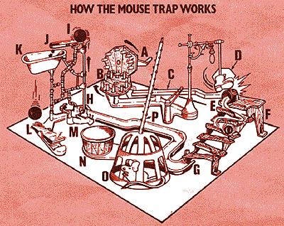
Do you remember the Mousetrap board game (above)? The arm hits the boot, which flies up and kicks over the bucket, which then tips over to release the ball and so on. It all works…just. But what happens if the bucket is on its side when the boot tries to kick it? The answer is, of course, that the boot will miss the bucket and the mouse will get away!
Now consider, if you will, the Bucket Brigade used in the early days of fire-fighting. The brigade forms a chain from the water supply to the fire. Each member in the chain waits for his left-hand neighbour to pass him a full bucket. He then turns to his right-hand neighbour and waits for him to take the bucket from him. If there is a hold up at the head of the chain (perhaps the fire has been put out), then each member in the chain will hold onto his current bucket until his neighbour can accept it. He does not simply release the bucket anyway (resulting in its falling to the floor). Similarly, if the well dries up, each member of the chain will stop once the supply of buckets is exhausted. He will not carry on miming the action of passing on invisible buckets! By this means, the whole interlocking chain is self timing.
Digital circuits often use handshaking to achieve this level of robust operation. Think of data as being analogous to the buckets. Control signals (usually request and acknowledge) provide the flow control.
Other circuits, by contrast, are more akin to the Mousetrap game. Such circuits will work, with a following wind, but their operation is less reliable. In particular, they will often fail in unspecified ways and may not be capable of graceful recovery from such occurrences.
The bad UART example (DUFF.vhd) has a good example of how not to do it thus:
A pulse is generated on signal checkStopBit when the RxState machine hits state CHECK_STOP_BIT. The Receive Shift Register sees this pulse and cheks the stop bit (which is present in RxShiftReg(8)) and assigns RxError as appropriate. The RxState machine then assumes that RxError will have been correctly assigned by the time it reaches state ON_ERROR (in exactly the same way that the Mouse Trap boot kicks the bucket on the assumption that it will be there). To compound the misdemenour, it became necessary to add a bodge in the form of RxErrorEarly (like RxError but decoded combinatorially) to avoid having to add yet another extraneous wait state. All in all, a pretty poor, though sadly typical implementation.
Two better alternatives to this implementation:
- Incorporate the check in line like the good example.
- Make the interface between the two clocked processes bomb proof by using Handshaking. The former solution is much to be preferred.
One error that is frequently seen, and make no mistake it is an error, is to declare memory-mapped registers and then split them up into fields, perhaps something like this:
reg [15:0] status;


  assign enable      = status[0];

  assign packetSize = status[7:1];

  assign errorFlag   = status[8];


    ....
// Read/write bus functionality.

  if( read ) then


      readData = status;


  if( write ) then


      status = writeData;
....
// Functionality associated with the purpose of the device.

  if( someErrorCondition )

          status[8] = 1'b1;
// Behaviour tied into address map...bad!
This way of writing code inevitably results in unwieldy and very inflexible code, principally because it is necessary to index into the registers all over the place. Even a simple change like moving a field into a different register becomes a major modification. It is also very difficult to deal tidily with unused bits, especially if they happen to have been defined in the middle of a given register. To make some bits read/write whilst others remain read only is almost impossible.
The correct approach is to declare each field individually and then concatenate them into registers as necessary, i.e. when they are written and read.
reg       enable

  reg [7:1] packetSize = status[7:0];

  reg       errorFlag;


    ....
// Read/write bus functionality.

  readData = 0;
// default

  if( read ) then

    begin


      readData[8]   = status;


      readData[7:1] = packetSize;


      readData[0]   = errorFlag;


      errorFlag     = 1'b1;
// Want a read/clear bit, no problem.

    end


  if( write ) then


      packetSize = writeData[7:1];
// Only this field is writeable.
....
// Functionality associated with the purpose of the device.

  if( someCondition )


      error = 1'b1;      // Independent of the address map...good.
The beauty of this approach is that the normal functionality of the module can be written unhindered by the constraints of the mapping of the various fields into the memory-map. Consequently, the memory map remains flexible and may be changed without having to touch the real module behaviour. The UART example (RTL.vhd) goes even further and doesn't even bother to declare the individual memory-mapped bits at all. The effect of reading and writing the various registers is simply applied straight to the state machines with no intermediaries.
The bad UART implementation (DUFF.vhd) makes the mistake of concatenating the three status registers TxReady, TxError & TxReady into a single signal called status(2 downto 0).
It is quite common to see circuits where a clever bit of circuitry is produced to generate timing pulses which are synchronised in some way to an incoming data stream. Those pulses are then used by a subsequent circuit to pick off the data. Such circuits can be made to work but they are hardly elegant and not very robust. They rely on timing to keep things ticking over smoothly. A much better approach is to take timing out of the picture whenever possible.
|
0 |
1 |
0 |
0 |
0 |
1 |
1 |
1 |
|
|
1 |
d0 |
d1 |
d2 |
|
|
|
|
|
|
1 |
|
|
|
|
|
|
|
|
|
1 |
|
|
|
|
|
|
|
|
|
1 |
|
|
|
|
|
|
|
|
|
1 |
|
|
|
|
|
dn-2 |
dn-1 |
dn |
Table 2 Frame Alignment Pattern
For example, imagine a circuit whose function is to detect a framing pattern from an input data stream, synchronise to it, and them extract the payload. This type of circuit is quite common in telecommunications applications. Such a pattern is given in Table 2. The repeating pattern begins with a frame alignment word (47h). Each subsequent byte is preceded by a binary 1. A state machine, an embedded counter and a large case statement can easily be written to align to such a pattern and then continously verify the pattern in order remain aligned.
A typical approach might be to tap off the incoming data stream with a synchronising circuit. That circuit would then produce a train of pulses that, hopefully, align with the incoming data. Said pulses would then be used by the subsequent circuit to pick the data out from the framing pattern. The danger with this approach is that any misalignment between data and its identifying pulse would lead to the wrong data being accepted and processed by the following module.
A more robust approach would be to pass the data right through the frame alignment module using the encapsulated data flow techniques described earlier. Input and output would make use of handshaking (which takes care of any variability in data rate). The function of the frame alignment module would be to annotate the data with an identifying flag (or perhaps frame count). Data and annotation would always be output together so interfacing to the resultant output data stream is simplicity itself (compared to the untidy interface resulting from the first method).
The short answer to this question is no. Statements are sometimes heard like, "it’s all very well writing RTL at a behavioural level, but the synthesiser will not do such a good job". The fear is that circuits designed in such a way will be either bigger or slower. I’ve even heard arguments to the effect that the synthesiser won’t understand such idioms and, therefore, will produce functionally incorrect net-lists.
My reply to the former problem is twofold. Firstly, does it matter? So what if a circuit is fractionally larger. Gates, nowadays, are cheap. Ok, so there are times when it is important not to exceed a particular die size and incur the cost and possibly extra design time entailed. That said, there is no reason for circuits designed at a high level of abstraction to be either bigger or slower. If two circuits are functionally identical, however they are coded, then the synthesiser will produce identical finished results. That said, designing for maximum robustness might add gates in some cases but that would be the case whatever the coding technique; it’s just easier to do at a behavioural level.
Few people realise just how powerful industry standard synthesisers like Synopsys and LeonardoSpectrum actually are. Basically, so long as the rules for producing synthesisable code are adhered to, then the designer may use of any of the powerful idioms described earlier with complete alacrity. If there are problems, they will be in terms of timing. Clearly, for example, deeply nested loops will map onto deep blocks of combinatorial logic. If the critical path of such a block exceeds the clock cycle period (less set-up and hold times as appropriate), then it is time to re-jig the design, perhaps by adding pipe-line functionality. That is why a trial synthesis of any complex logic should be carried out at an early stage in the design cycle (even before the code has been functionally de-bugged). That is something experienced designers do as a matter of course. It is always possible to write code with suitable behaviour. But it is cannot easily be known in advance whether that code will synthesise to produce a fast enough circuit.
Incidentally, both UART implementations were synthesised with the following results:
Good implementation: 50 registers, 101 gates, total 151;
Bad implementation: 64 registers, 90 gates, total 154.
We can see that working at a high level of abstraction does not absolve the designer of the responsibility to think about the gates that his code will actually produce. What it does is allow him the freedom to think in terms of what the design has to do, rather in the way a software engineer would. RTL may be written with a lightness of touch not possible using conventional make join techniques (to borrow a metaphor from an early HDL known as ELLA). Not all designers will agree with this article (stirring up a bit of controversy was part of the point of writing it) and still fewer will actually become exponents. Nevertheless, I contend that these techniques add power to the designer’s armoury that should not be dismissed lightly. At the very least, the article should stimulate a bit of thought.
Appendix: Table of VHDL/Verilog equivalent constructs
|
VHDL |
Verilog |
||
|
Terminology |
Description |
Terminology |
Description |
|
variable |
|
reg |
|
|
signal |
|
reg |
|
|
:= |
Variable Assignment |
= |
Blocking Assignment |
|
<= |
Signal Assignment |
<= |
Non-blocking Assignment |
|
entity |
Used to define a single stand-alone design unit. |
module |
Equivalent to a combined VHDL entity/architecture. |
|
architecture |
Used to define the contents of a given entity. A single entity may have multiple architectures. |
|
|
|
process |
Repository within which a block of sequential code is written. |
always block |
As VHDL process. |
|
function |
|
function |
|
|
procedure |
|
task |
|
|
|
There is no VHDL equivalent construct. This is the single biggest disadvantage of VHDL with respect to Verilog. |
fork/join |
Run two or more threads in parallel within a sequential block. |
|
record |
A construct that allows related declarations to be grouped together and handled as a single entity. Similar to the structure in ‘C’. |
|
There is no Verilog equivalent to this; though it can be quite easily emulated. |
Table 3 Useful VHDL/Verilog equivalent constructs