System 09 - VHDL 6809 System On a Chip
System09 is instruction set compatible with the 6809 and now runs the Flex 9 operating system. It includes a 2KByte KBug monitor program along with a UART and simple timer, parallel I/O port and hardware bus trigger for debug purposes. Along the way I have added a PS/2 keyboard interface and 80x25 character Video Display Unit.
The following file is for the Burch ED B5-X300 board which uses the XC2S300E Spartan 2e FPGA. I have removed all the old versions of System09 to save web space. (I only have 10MBytes of disk space for the web page). There is also a version for the Digilent Spartan 3 Starter board.
30th December 2006
A discussion mailing has been set up for System09 users to exchange ideas.
The web site for the mailing list is:
http://lists.bknr.net/mailman/listinfo/system09
Many thanks go to Hans for setting it up for me.
Latest Snapshot 2007-07-15 (still a work in progress)
All the board implementations are included in this Zip file.
System09_2007-07-15.zip
See revision log 15th July 2007
Sys09-vdu-B5-X300.zip
Revision Log of Latest Release 11th July 2006
6809 Software for System09
motasm.zip - Motorola 68xx assemblers written in C
AS09_DWC_211.zip - Improved 6809 assembler by Don Coates.
Sbug9.zip - 6809 monitor program (SWTPC compatible)
kbug9s_2004-09-11.zip - 6809 monitor program with VDU driver for System09
S1 Dump of Flex9
S1 Dump of XBasic
Flex9sys.zip - Disk images, RAM disk downloader and Flex9 binary
http://www.noicedebugger.com/ - NOICE Debugger by John Hartman
NOICE_2006-07-04.zip - NOICE ROMS for System09 (with permission from John Hartman)
John Hartman has kindly made the NOICE debugger for the 6309/6809 free if you e-mail him a description of what you are doing with a 6809 (in homage to a great processor).
http://www.oddchange.com/gcc6809/ - C Compiler for the 6809 by Brian C. Dominy
ADM3A_2006-07-16.zip - ADM3A terminal emulator for System09 written in gcc6809.
The ADM3A terminal emulator has been compiled using gcc6809 version 3.4.5 (?) running under cygwin. The version of gcc6809 I was given had problems with the frame pointer so it was necessary to use the "-fomit-frame-pointer" on the compiler. I believe the problem is now fixed or will be fixed shortly (as of 16th July 2006). The ADM3A terminal emulator needs some start-up assembler code to initialise the stack pointer before calling main(). The entry point is "_startup". You will need to look up the address in the ".map" file or use NOICE and "Play" the ".NOI" file and then look up the label. Note that you cannot single step the ADM3A terminal emulator in NOICE as it shares the serial port in system09 and will crash NOICE. You can however enter text through the NOICE command window when the terminal emulator is running.
System09 Memory Map:
This is the memory map I have attempted to maintain for different board implementations. I have tried to maintain consistency with the SWTPc (South West Technical Products Computer) memory map.
$00000 - $FFFFF RAM (Overlayed by I/O & ROM) $XE000 - $XE7FF(1) I/O $XE800 - $XEFFF(1) RAM / External Bus $XF000 - $XF7FF(1) Monitor ROM Extension / RAM / DMAF-2 (SWTPC) $XF800 - $XFEFF(1) Monitor ROM $XFF00 - $XFFFF(2) Monitor ROM / Dynamic Address Translation Registers (1) Physical Address bits PA[19..16] generated by the DAT are not decoded
(2) Logical Address Range $FF00 to $FFFF is not mapped through the DAT.
Dynamic Address Translation ($FFXX):
The Dynamic Address Translation Registers extends the addressing range of the 6809 to 1MByte by mapping the top 4 address lines of the 6809 through a 16 register 8 bit look up table to generate 8 Physical Address lines. This allows any 4KByte memory block in the 6809 Logical Address range to be mapped into any 4K memory block of the 1MByte Physical Address range. The bottom 4 Physical Address lines are inverted out of the DAT to be compatible with the SWTPc MP-09 CPU Board. Also address range from $E000 to $FFFF is not decoded using the top 4 Physical Address lines. Address range $FF00 to $FFFF is not mapped through the DAT. A read performed in this range reads the monitor ROM, a write sets the DAT registers, so the top 256 bytes of the monitor ROM can be used to configure the DAT on reset.
$FFF0 Memory Page $0XXX $FFF1 Memory Page $1XXX $FFF2 Memory Page $2XXX $FFF3 Memory Page $3XXX $FFF4 Memory Page $4XXX $FFF5 Memory Page $5XXX $FFF6 Memory Page $6XXX $FFF7 Memory Page $7XXX $FFF8 Memory Page $8XXX $FFF9 Memory Page $9XXX $FFFA Memory Page $AXXX $FFFB Memory Page $BXXX $FFFC Memory Page $CXXX $FFFD Memory Page $DXXX $FFFE Memory Page $EXXX $FFFF Memory Page $FXXX
DAT Register Value:
Bit[7] Bit[6] Bit[5] Bit[4] Bit[3] Bit[2] Bit[1] Bit[0} PA19 PA18 PA17 PA16 PA15* PA14* PA13* PA12* PA = Physical Address
PAxx* = Inverted Physical Address
I/O Memory Map:
Note that not all board implementation have all the peripherals implemented. By maintaining a consistent memory map, I/O drivers can be easily used on different board implementations with out the need to redefine I/o addresses.
$E000 ACIA $E010 Reserved for Floppy Disk Controller (SWTPc) $E020 PS/2 Keyboard $E030 80 x 25 character VDU $E040 Compact Flash $E050 Timer $E060 Bus Trap Logic $E070 Parallel I/O port $E080 Reserved for 6821 Printer/Counter PIA (SWTPc) $E090 Reserved for 6840 Programmable Timer Module (SWTPc) ACIA Registers ($E00X)
$E000 Command / Status Register $E001 TX / RX Data Register ACIA Status Register ($E000 Read)
Bit[7] Bit[6] Bit[5] Bit[4] Bit[3] Bit[2] Bit[1] Bit[0} IRQ PErr OErr FErr CTS DCD TxBE RxDR
Bit[7] - IRQ - Interrupt request
Bit[6] - PErr - Receive Parity error (parity bit does not match)
Bit[5] - OErr - Receive Overrun error (new character received before last read)
Bit[4] - FErr - Receive Framing Error (bad stop bit)
Bit[3] - CTS - Clear To Send level
Bit[2] - DCD - Data Carrier Detect (lost modem carrier)
Bit[1] - TxBE - Transmit Buffer Empty (ready to accept next transmit character)
Bit[0] - RxDR - Receive Data Ready (character received)
ACIA Control Register ($E000 Write)
Bit[7] Bit[6] Bit[5] Bit[4] Bit[3] Bit[2] Bit[1] Bit[0} RxIEnb TxCtl(1) TxCtl(0) WdFmt(2) WdFmt(1) WdFmt(0) BdCtl(1) BdCtl(0) Bit[7] - RxIEnb
-- 0 - Rx Interrupt disabled
-- 1 - Rx Interrupt enabled
Bits[6..5] - TxCtl
-- 0 1 - Tx Interrupt Enable
-- 1 0 - RTS high
Bits[4..2] - WdFmt
-- 0 0 0 - 7 data, even parity, 2 stop
-- 0 0 1 - 7 data, odd parity, 2 stop
-- 0 1 0 - 7 data, even parity, 1 stop
-- 0 1 1 - 7 data, odd parity, 1 stop
-- 1 0 0 - 8 data, no parity, 2 stop
-- 1 0 1 - 8 data, no parity, 1 stop
-- 1 1 0 - 8 data, even parity, 1 stop
-- 1 1 1 - 8 data, odd parity, 1 stop
Bits[1..0] - BdCtl
-- 0 0 - Baud Clk divide by 1
-- 0 1 - Baud Clk divide by 16
-- 1 0 - Baud Clk divide by 64
-- 1 1 - ResetPS/2 Keyboard Registers ($E02X):
$E020 Control / Status Register $E021 Tx / Rx Data Register Keyboard Control Register ($E020 Write)
Bit[7] Bit[6] Bit[5] Bit[4] Bit[3] Bit[2] Bit[1] Bit[0} RxIE CRB6 - - - - - - Bit[7] - RxIE - Receive Interrupt Enable
Bit[6] - CRB6 - Control Register Bit 6 (no function)
Bit[5..0] - Undefined
Keyboard Status Register ($E020 Read)
Bit[7] Bit[6] Bit[5] Bit[4] Bit[3] Bit[2] Bit[1] Bit[0} RxIRQ CRB 6 TxErr ShftOn KeyRel KeyExt TxDE RxDR Bit[7] - RxIRQ - Receive Interrupt Request
Bit[6] - CRB6 - Control Register Bit 6 (no function)
Bit[5] - TxErr - Transmit Error - No keyboard detected
Bit[4] - ShftOn - Keyboard Shift On
Bit[3] - KeyRel - Key Released
Bit[2] - KeyExt - Key Extended
Bit[1] - TxDE - Transmit Data Empty
Bit[0] - RxDR - Receive Data Ready (Valid data in receive register)
VDU Registers ($E03X):
The VDU is a text based display with 2K bytes of text buffer memory and 2K bytes of character attribute memory designed to run with a high resolution PC video monitor.
The VDU is permanently configured for 80 characters across by 25 characters down. It supports 8 foreground colours and 8 background colours and also supports alternating flashing characters and a chunky graphics character mode.
Pixel Clock = 25 MHz
Horizontal Pixels / Character = 8
Horizontal Display Characters = 80
Horizontal Sync Period = 3.84 usec
Horizontal Sync Frequency = 31.25 KHz
Vertical Lines / Character = 16
Vertical Display Characters = 25
Vertical Sync Pulse Period = 32 usec
Vertical Sync Frequency = 70 Hz (approx)
Please ensure your video monitor is capable of supporting this format before using it with System09. No responsibility is taken for damage to your monitor if it does not meet these specifications (or even if it does for that matter).
A flashing cursor is displayed at the Cursor Column and Row position. The Cursor Column position must be modulo 80, and the Cursor Row position should be modulo 25. The process of writing a character to the screen is to set the Cursor Column and Row coordinate then write the Character attribute byte, then the ASCII character code to the Write Character register. The value of the Write Attribute register is preserved so writing to the Write Character register will use what ever value was previously stored in the Write Attribute register.
The display can be scrolled up or down using the Row Display Offset. The Row Display Offset sets the starting address in the text buffer and attribute buffer memory. When the display is scrolled up or down, the Row Display Offset should be rounded modulo 25. The Cursor Column and Row position is relative to the screen position with the 0,0 coordinate being at the top left of the screen.
$E030 Write Character (at cursor) $E031 Write Attribute (colour - RGB foreground & background) $E032 Cursor column position (0-79) $E033 Cursor row position (0-24) $E034 Row Display Offset (0-24)
VDU Attribute Register ($E031):
Bit[7] Bit[6] Bit[5] Bit[4] Bit[3] Bit[2] Bit[1] Bit[0} Graphics BG Blue BG Green BG Red Blink FG Blue FG Green FGRed
I'm not sure this is 100% accurate but you get the idea.
In graphics mode, (Graphics bit set) characters represent a 8 pixel graphics characters and are displayed as follows:
Bit 0 Bit 1 Bit 2 Bit 3 Bit 4 Bit 5 Bit 6 Bit 7 Compact Flash Registers ($E04X):
$E040 Data Register $E041 Error/Feature Register $E042 Sector Count Register $E043 Sector Number Register / LBA[7..0] $E044 Cylinder Low Register / LBA[15..8] $E045 Cylinder High Register / LBA[23..16] $E046 Head Register / LBA [??..24] $E047 Command / Status Register Timer Registers ($E05X):
$E050 Read - Down Count $E050 Write - Preset Count $E051 Read - Status $E051 Write - Control Timer Control Register
Bit[7] - interrupt enable
Bit[6..2] - undefined
Bit[1] - mode (0 = counter, 1 = timer)
Bit[0] - counter enableTimer Status register
Bit[7] - interrupt flag
Bit[6] - timer output
Bit[5..0] - undefined
Trap Logic Registers ($E06X):
$E060 Address Comparator High Byte A[15..8] $E061 Address Comparator Low Byte A[7..0] $E062 Data Comparator D[7..0] $E063 Control Comparator VMA, R/W $E064 Address Qualifier High Byte A[15..8] $E065 Address Qualifier Low Byte A[7..0] $E066 Data Qualifier D[7..0] $E067 Control Qualifier VMA, R/W Address, Data and Control signals must match in the Comparator registers
Matches are qualified by setting a bit in the Qualifier registers
Trap Control Comparator (write)
Bit[7] - Match polarity 1=match 0=mismatch
Bit[6..2] - undefined
Bit[1] - VMA
Bit[0] - R/W 1=read 0=write
Trap Control Qualifier (write)
Bit[7] - Interrupt Enable
Bit[6..2] - undefined
Bit[1] - VMA 1=valid 0=don't care
Bit[0] - R/W 1=valid 0=don't care
Trap Control Qualifier (read)
Bit[7] - Match flag
Parallel I/O Port Registers ($E07X):
$E070 Data I/O Register A $E071 Data I/O Register B $E072 Data Direction Register A $E073 Data Direction Register B
System09 Revision Log
20th March 2003
Interim Snap Shot .
30 March 2003
Snap shot of a 6809 design as of 30th March 2003 uses 109% of slices in an XC2S200 FPGA so does not compile. It includes a 2K Monitor ROM which is probably what is taking up all the LUT's
The 6809 is currently missing the following features
1. No FIRQ
2. No SWI2 or SWI3 although it does decode those op codes
3. E Flag (Entire) does not prevent stacking of registers
I have replaced the parallel I/O port with Compact Flash support using the B5-CF module in 8 bit IDE mode
29th April 2003
It does not appear to work at this stage, although the test bench seems to indicate it should print out the "Hello World" message to the UART. Using the Hello World test ROM in place of the Boot ROM does not appear to work.
I have removed the 2K SBUG9 monitor ROM and included a 256 byte ROM which should Boot SBUG9 from Compact Flash. The 256 byte ROM is mapped at the top of memory on reset. On reset, the boot ROM should copy itself to RAM, then boot an Image of SBUG from the B5-CF Compact Flash into write only RAM at $F800 - $FFFF before switching the ROM out and making the RAM at $F800-$FFFF read only.
On reset, The ROM is mapped at $FF00 and a write to $F800 - $FFFF write to shadow RAM. By writing to location $E030, the ROM should be mapped out, and the Monitor RAM is made Read Only. A Write to $F800-$FFFF will then write to the Dynamic Address Translation registers.
The 256 byte boot ROM configures the B5-CF Compact Flash module for 8 bit LBA mode. The Boot ROM should load 4 x 512 byte sections containg SBUG at LBA Address $0F47C - $0F47F. You need to use the Compact Flash sector write routines (cf.zip) with the System68 design to write an image of SBUG to the Compact Flash.
So far as I can tell, the Compact Flash is being accessed as the activity led blinks shortly after the release of Reset. I've tried implementing the Compact Flash boot in a known working CPU design on the board (System68) but that does not work either. System68 works fine with internal ROM, but will not boot SWTBUG out of compact flash using the same boot ROM switch as the System09.
The System09 design uses 97% of Slices in an XC2S200 FPGA, so its a tight fit .... It would be good to have a B5 board with 300K gates as I could then include the SBUG ROM in the FPGA.
I've implemented FIRQ, and the E (Entire) bit, and SWI2 and SWI3 missing on the previous snapshot. One of the Test Benches should exercise all the Software Interrupts. I've also modified the PSH/PUL instructions so they only execute cycles when there is a register to be pushed or pulled.
29th June 2003
Hans Pufal has suggested that I make use of block RAM so that I can fit the SBUG monitor ROM into the FPGA with the CPU. this eliminates the need to boot the monitor ROM image from Compact Flash. So far I have not managed to get the block RAM working as a ROM. Refer to the System68 design for a further discussion on the use of block RAM. With the Slice test ROM installed the CPU spits out 13 x " ' " or 0x27 characters. This is the exact number of characters in the "Hello World\d\n" string. I can find nothing in the simulation that explains this. The CPU seems to be working fine in the behavioural simualtion, so I suspect there is a timing issue to contend with.
I have fixed a few bugs in the state sequencer with this snapshot.
19 July 2003
Prints out "Hello World"
After a bit of a break, I have got back into the 6809 design and found a bug in the MiniUART. Now it prints out "Hello World". Wooo Hoo !!!! I have been advised that NMI's should be disabled until the S Stack pointer has been set up with an LDS or LEAS. I have yet to implement that suggestion.
5 September 2003
Works with SBUG Monitor ROM
Well it appears to work .... Tony Burch has loaned me a B5_X300 which has given me enough space to include a 2 K Slice ROM. Note however that I am still using a modified B3_SRAM board and the B3_FPGA_CPU_IO module. If you are using Tony's latest B5 modules, you will have to update the User Constraint File to reflect the new pin out.
There are some issues with regard to clock edges. I thought the CPU clocked on the falling edge of the system clock but it appears, after simulating the entire system, to clock on the rising edge. I have not done it on this version, but I need to change the clock edge so that I can use alternate clock phases on the block RAM. I did manage to get System68 to read Block RAM ROM by reversing the clock edge. It appears I was gating the write on the first half of the cycle rather than the second half, which explained the problems I was having. It certainly helps to simulate the design properly.
There were a few bugs I found in the core:
-- Fixed 16 bit indexed offset, It was doing reading the offset at the EA rather than fetching it at the PC address
-- Added/Fixed STY and STS instructions - STY and STS was not decoded correctly in the second page decode state
-- ORCC_STATE ANDed CC state rather than ORed it - Now fixed
-- CMPX Loaded ACCA and ACCB - Now fixed
I've also cleaned up the component end entity syntax. The Modeltech simulator is much more fussy about synctax than the XST VHDL synthesis tools.
There are bound to be more bug fixes, so stay tuned for any updates.
6th September 2003
Initial Open Cores version
This is a screen of the version released to the open cores web site on 6th September 2003. It should be the same as the version above, except I commented the code a bit more.
16th September 2003 3:10 am AESTNow using Block RAM
I finally got the Monitor Program running in Block RAM. This version uses 81% of the slices of a XC2S300e. The version with Slice 2KByte ROM uses 3070 out of 3072 slices so it was a pretty tight fit. I thought the ROM would use more slices than it does.
Device utilization summary:
Number of External GCLKIOBs 1 out of 4 25%
Number of External IOBs 83 out of 142 58%
Number of LOCed External IOBs 83 out of 83 100%
Number of BLOCKRAMs 4 out of 16 25%
Number of SLICEs 2494 out of 3072 81%
Number of GCLKs 1 out of 4 25%
I'm now using a B5-SRAM module and the B5-Peripheral-Connectors Modules with the B5-X300 FPGA board. The B5-SRAM is installed on connectors E & F, I'm using the B5-Peripheral-Connectors on connector C and I have the B5-CF Compact Flash installed on connectors A & B. The UCF file should contain all the relevant pinouts. The Clock is Running at 9.8 MHz or so (I think) and the baud rate is 9600Bd.
--------------------------------------------------------------------------------
Constraint | Requested | Actual | Logic
| | | Levels
--------------------------------------------------------------------------------
TS_sysclk = PERIOD TIMEGRP "sysclk" 100 | 100.000ns | 56.524ns | 11
nS LOW 50.000000 % | | |
--------------------------------------------------------------------------------
TIMEGRP "ram_cs" OFFSET = OUT 40 nS AFTE | 40.000ns | 35.583ns | 14
R COMP "sysclk" | | |
--------------------------------------------------------------------------------
TIMEGRP "ram_wr" OFFSET = OUT 40 nS AFTE | 40.000ns | 31.006ns | 11
R COMP "sysclk" | | |
--------------------------------------------------------------------------------
TIMEGRP "ram_addr" OFFSET = OUT 40 nS AF | 40.000ns | 36.781ns | 13
TER COMP "sysclk" | | |
--------------------------------------------------------------------------------
TIMEGRP "ram_data" OFFSET = OUT 40 nS AF | 40.000ns | 35.755ns | 11
TER COMP "sysclk" | | |
--------------------------------------------------------------------------------
TIMEGRP "ram_data" OFFSET = IN 15 nS BEF | 15.000ns | 12.610ns | 5
ORE COMP "sysclk" | | |
--------------------------------------------------------------------------------
TIMEGRP "test_alu" OFFSET = OUT 90 nS AF | 90.000ns | 55.967ns | 22
TER COMP "sysclk" | | |
--------------------------------------------------------------------------------
TIMEGRP "test_cc" OFFSET = OUT 95 nS AFT | 95.000ns | 63.168ns | 24
ER COMP "sysclk" | | |
--------------------------------------------------------------------------------
| 50ns | 50ns |
SysClk -----\___________________/--------------------\________ (10MHz)
| 37ns |
ram_addr ----------------<==================================>---
| tacc = 50ns > 15ns | 13ns |
ram_data --------------------------------------<==========>---- (read)
The conclusion is, you could probably shave 20nsec off the cycle time and it would still work reliably. ie. should run at 12.5 MHz. It would depend on the required set up time of the block RAM which clocks the address and data on the rising clock edge.
29th November 2003 release B.
This version corrects some errors in indexed addressing. ACCA and ACCB indexed offset should be 2's complement. I have now sign extended them in the Right ALU mux. Also absolute indirect addressing had an error in the bus cycle for for picking up the low byte of the 16 bit absolute address. It performed a read rather than a fetch cycle. It has now been fixed.
The errors were picked up by a more comprehensive test of addressing modes, using TESTBENCH5.VHD. I can now execute a SWI in a program and CPU09 will return to the monitor program correctly.
29nov03b fixes up the problem with breakpoints. I assumed the LEA instructions did not affect the condition codes. In fact LEAX and LEAY affect the Z flag. LEAS and LEAU do not affect any condition code flags. SBUG relied on an LEAY -3,Y to clear the Z Flag. I've added an extra ALU control function "alu_lea" which does the same thing as the "alu_ld16" (16 bit load) but only affects the Z condition code.
It was also suggested to me sometime back that interrupts should be disabled until the S stack pointer is loaded either with an LDS or LEAS instruction. I have still yet to do that.
I'm now using WebPack ISE 6.1. They have made a number of changes, and now I am not sure what they have done with the User Constraint File.
12th December 2003
Fix on CWAI. Microcode did not push the return state before masking the Condition Codes - Thanks to Ghassan Kraidy for picking up this fault.
17 January 2004
CLR fix, Updated UART.
The CLR instruction did not clear the carry flag. This was picked up by Michael Hasenfratz. It affected a number of CPUs in the SystemXX range. It was due to an error in the ALU control in the state sequencer.
I've also updated the miniUART so that it supports synchronous X1 clock inputs. I've also added CTS control of the transmitter and DCD interrupts and receiver control.
I've updated the start bit synchroniser in the UART. There was a race condition on the start bit level detect and edge detect that resulted in unreliable operation. The UART now works reliably at 38.4 Kbaud.
26 January 2004
Numerous bug fixed
After an all night session I have XBASIC running on System09.
Bugs found are as follows:
1. PSHU was referencing the SP in one of the states
2. STD instruction did not set the condition codes
3. JMP direct was not implemented
4. CLR direct performed an addition read cycle which was not necessary
5. Bogus latch instruction prevented page2 indexed instructions from working
6. Minor alterations to microcode subroutine calls.
7. removed "test_alu" and "test_cc" signals to free up I/O ports.
8. TFR did some strange things to the condition codes, although should not have had any harmful effects
9. removed redundant "alu_inx" and "alu_dex" definitions
S1 Dump of Flex9
S1 Dump of XBasic
System09 runs at 38K4 baud with a 4.9 MHz (9.8 MHz ???) clock. (8 data 1 stop bit)
On reset you should get the SBUG message and a ">" prompt
Put SBUG in load S1 Load mode by pressing the "L" key
Send the F9.s19 file with Hyperterm in text download mode. (no handshake protocol is used)
Set the PC to $CD00 (<ctrl> P CD00)
Execute Flex by pressing the "G" key
Enter the date and you should get a +++ prompt
Return to SBUG by entering "MON" <enter>
Put SBUG in load S1 Load mode by pressing the "L" key
Send the XBASIC.s19 file with Hyperterm in text download mode.
Set the PC to $0000 (<ctrl> P 0000)
execute XBASIC by pressing the "G" key
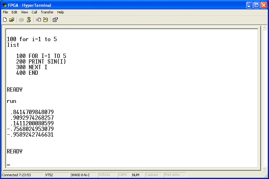
Type in a basic program.
Screen dump of XBASIC running under Flex9 (only runs console I/O at this stage)
1 February 2004
Runs Flex9 Operating System
Two basic bugs:
1. CWAI did not increment the program counter in one of the bus cycles
2. ABX was performing a signed addition rather than unsigned like it should have
I have added Bus trap logic that allows an NMI to be generated on any address, any data and any read/write and vma condition. this hardware is useful for trapping writes to specific memory locations. There is no documentation on it yet, so you will have to read the header of the VHD file to find out how it works.
I have written a RAM disk driver that uses the DAT and the top 192K bytes of RAM. It requires a disk geometry of 48 tracks x 16 sectors per track. I have used the Evenson SWTPC emulator and floppy disk maintenance tool to generate the required disk format. I used a "makehex" utility written in C to convert the binary disk image into a ASCII hexadecimal dump. I have written a RAM disk download utility for the 6809 called "ramdskdl" and I have overlayed my ram disk drivers on a binary copy of Flex9.
Flex9sys.zip - Disk images, RAM disk downloader and Flex9 binary
The procedure is as follows:
Download the Flex9.s19 binary image using the SBUG "L" command
Download the Ramdskdl.s19 binary image using the SBUG "L" command
Set the program counter to $1000 (<ctrl> P 1000)
Execute the program with the "G" key.
Ramdskdl will prompt you to download the disk image
Being careful not to press any keys on hyperterm, send the Flex hexidecimal disk image "flex9sys.hex" as a text file. This will take a few minutes. The file must be exactly the right length for this to work and there is no error checking on the file.
If the download is successful the program will send a message to say the download is complete and jump off to Flex9. Flex9 will then prompt for the date as MM,DD,YY. Note that Flex9 is not Y2K compliant.
Once you have the "+++" prompt you can type in commands such as "DIR" or "CAT" to list out the files on the RAM Disk. There are two basic interpreters "BASIC" and "XBASIC" there is a 6809 macro assembler "ASMB" and a line editor "EDIT". There is a modem program for uploading and downloading files "MODEM69", but I'm not sure what protocol it uses and if it needs a secondary serial port.
Note that at the moment there is no way to upload the disk so any work you do on the RAM Disk will be lost.
There is a utility for running remote disks over a serial link called NetPC also available on the Evenson web site but I have not implemented that yet.
4th April 2004
Added PS/2 Keyboard and 64 x 32 VDU
PS2 keyboard is from open cores (I think) and has been translated from Verilog to VHDL. I have set it up to look like a receive only 6850 ACIA, with a few extra bits. It outputs ASCII coded characters. Key scan codes can be implemented by removing the comments and adding an extra register.
The VDU runs at 64 characters across x 32 rows down. It uses a pixel clock of 25MHz, a line frequency of 39KHz and I'm not sure what the field rate is.
I have to write a new monitor ROM that has the terminal drivers and keyboard interface.
21 Nov 2005
Improved 80 x 25 VDU, 50MHz System Clock, KBug9 Monitor ROM
This version takes the improved Keyboard and VDU developed for the Spartan3 Starter Board and implements then on the Burch B5-X300 board. KBug9 source and Don Coates 6809 assembler are available on the Spartan3 page. Note that the I/O map has be re-arranged so that the KBug Monitor ROM with Video Driver will run on the system.
The ICS525 PLL system clock should be configured for 50MHz. Note that the CPU still runs at 12.5MHz as the basic E Clock.
The VDU Attribute register now only supports 8 colours. This is to allow for a graphics attribute bit and a flashing character attribute bit. The Character generator is also now higher resolution than the previous B5-X300 version. The VDU runs at 80 characters across by 25 rows down. It uses a pixel clock of 25MHz. It is formatted at 640 pixels across x 400 pixels down. Total pixels across = 800, Total pixels down = 450
KBug9s includes basic video drivers. There is as problem when the offset Register exceeds 24. The Character columns get messed up. 2048 Byte buffer = 80 x 25 characters. Also It does not yet emulate the ADM-3A completely ... it is missing some of the control codes.
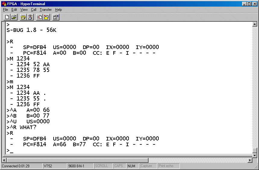
Some of the KBug9 commands are:
I [S/K] Enable Input device (Serial/Keyboard)
O [S/V/P] Enable Output device (Serial/VDU/Printer)
P [start]-[end] Punch S1 Tape
L Load S1 Tape
E [start]-[end] Dump Memory
M [addr] Memory Examine & change
R Dump registers
G [addr] Execute Program
S display S stack pointer & Dump registers on stack
^A AccA examine & change
^B AccB examine and Change
^C Condition Codes
^U Ustack pointer
^X X Index register
^Y Y index register
^P Program counter
20th Aug 2005
Bug Fix on LSR8
There is an error in the LSR8 instruction in CPU09. LSR8 was treated in the same way as LSR16, which was OK on the dual operand instructions as the high byte of ACCA and ACCB was set to zero on the left input to the ALU. For single operand instructions however, the data byte is read into the low byte of the MD (Memory Data) register and bit 7 is sign extended to the high byte. This was to support signed offsets in the branch instructions. This meant that the LSR8 instruction would operate like an ASR8 instruction with the sign bit being preserved. The fix was to place the ALU_LSR8 ALU operator with the ALU_ROR8 and ALU_ASR8 operators. This bug was spotted by an astute opencores user.
17 Sep 2005
Bug Fix on JSR, EXG CC and TFR CC
Two more bugs were brought to my attention.
The first was that EXG and TFR instructions did not work on the condition code register. Extra cases had to be assigned to the ALU to set the Condition Code output register to the Left ALU input for the ALU TFR operation.
The second problem was to do with JSR [0,S]. The indexed jump to subroutine pre-decremented the stack pointer ready to push the return address before the indexed addressing mode was calculated. This had the effect that JSR instructions indexed to the stack would get the wrong vector address. The solution was to defer the S Stack pointer decrement until after the indexed addressing mode microcode and add an extra cycle to the JSR microcode state. this required minimal effort. Note also that the JSR extended instruction gained an extra cycle as it shared the JSR microcode state.
12th Jun 2006Fixed Bug in ASR, LSR, ROR
Fixed bug in CLR
After some exhaustive testing of the single operand instructions, comparing an EF68A09 system to System09 on a Spartan 3E starter board, I found some errors in the ASR, LSR, ROR and CLR handling of the Overflow (V) Flag. ASR, LSR and ROR modify the V bit on the 6800, but not the 6809, so I had to disable the code in the ALU of CPU09 that modified the VFlag. Also the CLR instruction did not reset the V Flag. This is now fixed too.
7th July 2006
Fixed bugs in NMI.
CPU09 Version 1.13
Disable NMI on reset until S Stack pointer has been loaded. Added nmi_enable signal in sp_reg process and nmi_handler process.
11th July 2006
Fixed bugs in MUL, RTI, SYNC, DAA and Interrupt Processing of CPU09.
CPU09.vhd Version 1.14 - 11th July 2006
1. Added new state to RTI called rti_entire_state. This state tests the CC register after it has been loaded from the stack. Previously the current CC was tested which was incorrect. The Entire Flag should be set before the interrupt stacks the CC.
2. On bogus Interrupts, int_cc_state went to rti_state, which was an enumerated state, but not implemented anywhere. rti_state has been changed to rti_cc_state so that bogus interrupt will perform an RTI after entering that state.
3. Sync should generate an interrupt if the interrupt masks are cleared. If the interrupt masks are set, then an interrupt will cause the the PC to advance to the next instruction. Note that I don't wait for an interrupt to be asserted for three clock cycles.
4. Added new ALU control state "alu_mul". "alu_mul" is used in the Multiply instruction replacing "alu_add16". This is similar to "alu_add16" except it sets the Carry bit to B7 of the result in ACCB, sets the Zero bit if the 16 bit result is zero, but does not affect The Half carry (H), Negative (N) or Overflow (V) flags. The logic was re-arranged so that it adds the MD register or zero so that the Carry condition code is set on zero multiplicands.
5. DAA (Decimal Adjust Accumulator) should set the Negative (N) and Zero Flags. It will also affect the Overflow (V) flag although the operation is undefined in the M6809 Programming Reference Manual. It's anyone's guess what DAA does to V although I found Exclusive ORing Bit 7 of the original ACCA value with B7 of the Decimal Adjusted value and Exclusive ORing that with the pre Decimal Adjust Carry input resulting in something approximating what you find on an EF68A09P.
25 Feb 2007
New Directory Structure
In an attempt to rationalize the directory structure, I've created the following structure in the zip file:
System09
docThe idea is that a new directory can be created for each new FPGA board implementations and vendor specific components such as block RAM can go in a separate folder. Currently I have folders for 4K Bit Spartan 2 block RAM/ROMs and for 16K Bit Spartan3/3E Block RAM/ROMs.
rtlSpartan2 (RAM & ROMS)src
Spartan3 (RAMS & ROMS)
System09_BurchED_B3 (project files)
System09_BurchED_B5-X300 (project files)
System09_Digilent_3S200 (project files)
System09_Digilent_3S500E (project files)
System09_Xess_XSA-3S1000 (project files)
Testbench
VHDL (Common IP Cores)Flex9tools
KBug9
KBug9s
Noice
Sbug
Sys09bug
Tracebugas09
epedit
romdiskI have attempted to use generics to define operating clock frequencies and timing parameters in the keyboard and VDU. This is only a snap shot release and is still a work in progress. Only the B5-X300 and XSA-3S1000 versions have been synthesized so far, and even those are not guaranteed to work properly.
The project files have been implemented using Xilinx Webpack 7.1. The advantage of this is that they are small and they are upwards compatible with later versions of Webpack. Project files for Webpack 8.1 and onwards get very large and
2nd July 2007
Various Changes
Updated Sys09Bug to include RAM disk drivers. I have also added an XModem compatible downloaded for the RAM Disk. It appears to download a RAM disk image of Flex9 correctly using hyperterm although there appear to be problems with the disk image I am using. Sys09bug partially implements some of the features found in the MicroBox2000 found on the Flex User Group FTP Site. It includes vectorable disk drivers for each drive so it is possible to have 2 RAM disk drives as well as a Flexnet drive on a PC.
On the B5-X300 version, Flex must be loaded into memory manually due to the limited Block RAM in the Spartan 2. The B5-X300 version has a Compact Flash interface, and Sys09bug includes a CF disk boot although the CF drivers have not been implemented for Flex yet and I have yet to create a disk image for the CF with the appropriate bootstrap loader. It should be possible to used the extended memory as a RAM disk, although that feature has not been implemented yet.
On the Spartan 3 starter board Flex is stored in RAMB16 which is mapped into memory. It does not have a CF interface, although it may be possible to store a boot disk image in the configuration flash. It is designed to use the extended RAM as two RAM disks.
The XESS XSA-3S1000 I have added a timer, bus trap logic and IDE interface. I have managed to add 8 Kbytes of RAMB16 to run Flex. This was achieved by sacrificing the RAMB16 used for the colour attribute memory in the VDU and using distributed memory for the key map table in the PS/2 keyboard. There were already 2 x RAMB16 blocks left over in the previous version. All 24 RAMB16 block have now been used. As of 2nd July 2007 1:52am the design had not been tested. The SDRAM interface has yet to be implemented. Without cache, the SDRAM is very slow taking up to 8 clock cycles at 50 MHz to perform a read or write so it will slow the CPU down by a factor of 4.
The Spartan 3E starter board design has not been updated yet.
A big thank you to David Burnette who has sent me an updated version of the UART Baud clock generator that scales the size of the divider counter to match the baud rate. This has been implemented on most of the board support packages.
15th July 2007
Flex running on CF Card
No real changes in hardware, but a few software utilities have been added to support formatting and downloading Compact Flash disk images. A CF version of Flex9 is now running on the B5-X300 board.
Back to FPGA Page