The basic element of a purely synchronous design is the Dtype. We define this as a latch whose contents/value only change on a rising clock edge. On a rising clock edge, the contents of the latch become whatever was on its D input, and its outputs become this value and its complement. The state of the latch and its outputs are then held constant until the next rising clock edge.
The trick is to manipulate the input signal to this latch: to do all the clever logic in creating the D input.
Safe design practice dictates that the clock input should NEVER be manipulated: every Dtype in the whole design should receive exactly the same clock signal. So, for instance, if you want to stop the Dtype from updating with a new value then rather than disabling the clock, you should feed the output of the Dtype back onto its input so that its current value (its state) is latched into the Dtype by the next rising clock edge (ie the state is unchanged).
Similarly, the set and/or reset of the Dtype is achieved by changing the D input to the Dtype and not by using some other asynchronous inputs to a more complex Dtype module.
Our aim is to produce a shift register which can be:
The strategy is to design a single-bit module which can then be repeated and wired in series to produce a shift register of arbitrary length.
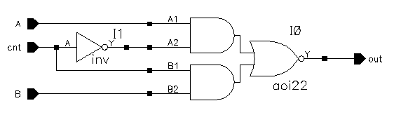
First, we design a multiplexor so that we can choose between either the input signal or the output signal (fed back) - this allows us to either shift in a new value or to hold the current value. The design below achieves this.
Notice that only two sub-modules are needed for this module since we are using a (slightly) complex gate: the and-or-invert gate.
                    cnt        out
                    --------------------
                    Low    inverse of A
                    High   inverse of B
We have designed the output of the multiplexor to be the inverted signal because: 1) the logic is simple; and 2) the signal will be inverted again by the logic which implements the reset.
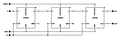
Below is the schematic for the shift-register module.

To understand the operation consider it in terms of: what value is on the D input?
To make a large shift register, we simply connect several of these modules together. Below is a three-bit shift register and the waveforms from a simulation to confirm its behaviour.
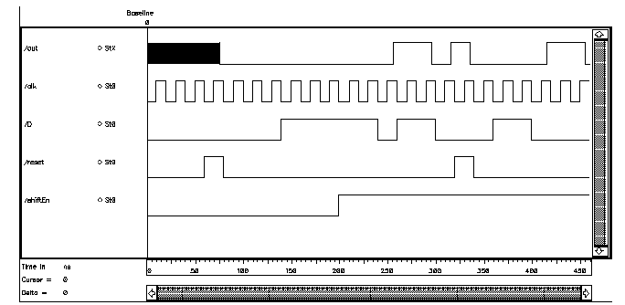
To understand the simulation output notice the following:
The binary counter is based upon the simple observation that a bit value changes (from 1 to 0, or from 0 to 1) only if all the bits of lower significance are ALL high.
                         0    0000
                         1    0001
                         2    0010
                         3    0011
                         4    0100
                         5    0101
                         -     - -
Thus all we need is to design is a bit module which either retains its value
or inverts it according to a control signal
(the AND of the lower bits). The module is known as a
toggle flipflop
and is shown below. Notice that it is almost identical to
the shiftCell designed above except that the inverted output is fed
back as the input to the multiplexor instead of a Data input.

Thus if the tog signal is Low, the state of the Dtype remains the same; if tog is High, then the state of the Dtype is inverted.
Below is the schematic for a four-bit counter with the least-significant-bit to the left.
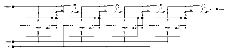
The counter is reset to zero by raising the reset signal. When the enable signal is Low, the counter does not change. When the enable signal is High, the counter increments by one on each rising clock-edge.

The simulation output above confirms this behaviour. Notice that the final output is raised when all the bits are High - and that the counter then returns to zero by itself. This can be seen more clearly in the enlarged plot region below.

The reset signals shown in these schematics are all a single input. However there may be both internal and external sources of resets. Indeed, when there is an internally generated reset signal, it is vital to remember the need to provide a global Reset to initialize the system.
For instance, the four-bit counter above could be enhanced into an 11-cycle counter (0 to 10) by using logic which recognizes the number 10 and generates a reset control signal. If this were connected directly to schematic's reset pin then it would simply reset the counter to 0 in the cycle after it reaches 10. However, there would be no way of starting the counter in a known value. Thus, the global reset and the internal reset should be combined with an OR gate to generate the schematic reset signal.