
Gerard M Blair, Department of Electrical Engineering, The University of Edinburgh, Scotland, UK
There are two skills which are essential to the digital designer:
This laboratory advocates a very rigid and prescriptive design discipline. There are many designers in the real world which ignore these rules. There are many designers who use them only when they "have to". There are some specific designs which can best be achieved without them. The techniques themselves depend upon the existence of an idealised globally distributed signal: the clock, which is sometimes impractical. However, synchronous design techniques give rise to rapid and safe design practices, particularly for designs which are contained within small areas of contiguous silicon - simple microchips are most simply implemented as synchronous design solutions.
The fundamental building block of this whole laboratory is the dtype. For our purposes we are going to define it as follows:
The dtype has 2 inputs, d and clk; and 2 outputs, q and q-bar. We talk about q as being the "value" of the dtype, and q-bar is its compliment. The outputs change only when the input signal clk rises from a low value to a high value. When the input clk rises, q becomes equal to the input d, and q-bar changes to their compliment. These values are then held until the next rising edge on the clk input. This is therefore known as a positive-edge triggered flip-flop.
Notice that this component has no asynchronous set or reset input signals as are commonly found with discrete components. The synchronous design philosophy abhors these: too many designs have failed due to spurious signals on these asynchronous inputs. The key to the success of synchronous design is that changes can only occur on a rising clk edge.
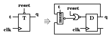
From this basic building block we build larger ones. At the moment we have a module which does nothing more than store its d input value and pass it on. A useful function to add to this would be a signal which (on the rising clk edge) causes the dtype to be set to a pre-determined value irrespective of its d input. Figure 2 shows two symbols and their corresponding schematics which achieve this. Notice that in both cases the q output on the symbol corresponds to the q-bar output of the dtype in the schematic. This is because the NOR and the NAND gates invert the d input to the new modules before it becomes the d input to the dtype - thus the inverted output of the dtype corresponds to the original input to the new modules. The two new modules differ in both the value which the control signal forces on to the dtype and also the value of the control signal which does the forcing. If a control signal causes an effect only when it is high, it is said to be active high; and correspondingly for low.
EXERCISE 1: Describe the function of these two schematics being careful to specify whether the control signals are active high or active low.


Another useful function is to be able to choose between two different inputs according to a control signal. Figure 3 shows a schematic for this function which uses a subcircuit known as a multiplexor. By adding a multiplexor before the input to a dtype we have a flip-flop whose input is selected according to the control signal.

EXERCISE 2: Using only NAND and NOT gates (and a little de Morgan) create a schematic which implements a multiplexor.
Figure 4 shows this circuit with one of the outputs of the dtype fed back to one of the multiplexor inputs.

EXERCISE 3: Describe the function which this schematic performs.
We now have enough information to do a simple design. The first trick with design work is to keep things as simple as possible; thus when you have a complicated schematic it is easiest to create a symbol with the equivalent inputs and outputs and to think of it purely in terms of the function it performs. The second trick is to think very carefully about the description of the full design and to break that down into a small number of simple sub-modules.
These two tricks are known respectively as bottom-up and top-down design. The best design practice starts with the functional description of what is to be implemented and breaks this down into smaller and smaller blocks until it is finally described in terms of the primitive modules which are already available; then these sub-modules are built up and connected (using the hierarchy established in the "breaking down") until the original function is implemented. The following should illustrate.
In the following, try to answer the questions and to perform the exercises before reading on. The answers appear later, but you will learn more by trying to find them yourself.
We wish to design an n-bit counter (say n=4) using purely synchronous techniques. In simple terms, the required module outputs a 4-bit binary number which increments on every rising clock edge. As specifications go, this was quite good. It has given you most of the information about the module - certainly all that the casual designer was really interested in. It does however leave out a practical issue: how do we start the counter from a known value?
As an engineer you must use your judgement when reading such a specification and suggest to the specifier that a reset signal should be included. For the purposes of this exercise, let us include the feature of a reset signal which sets the counter's output values to zero. What is still wrong with this specification?
Stage 1: Analyse the problem. Write down 0 to 15 in binary - this is best done in a column to see how individual bit values change. In synchronous design, the trick is to look at the information which is available at the state before the changes must occur. Can you see a pattern or clue which could be used for each bit of the counter?
In this problem, we can say that an individual bit will change in the next cycle if, and only if, all the bits to the right hand side of it are "1". This applies both to a bit going high and to a bit going low. Thus we have a condition at any given cycle by which we can determine the changes in the next.
Each bit can be implemented as a toggle: a dtype which either remains in the same value or changes to its opposite value according to a control signal. Notice, we have now broken the problem of a 4-bit counter into the design of a single bit cell, and some control logic.
Stage 2: Design a toggle flip-flop. For now let us ignore the need for a reset. Look back at Figure 4 and adapt it so that the value of the dtype can be inverted according to the control signal.
Note that in this design discipline you are not allowed to add any gates to the input clock signal. While it might be an attractive idea to simply disable the clock (and so prevent the dtype from changing), it is likely that such an approach would lead to spikes or glitches on the input clock line - and so to failure!
Figure 5 shows an implementation of a toggle with an (active high) reset signal. Notice that the multiplexor now has a small circle drawn on its output so that it represents an inverting multiplexor. This new function can we can describe as follows:
        if t is HIGH
           out is equal to the inverse of b (the top input signal)
        else (if t is LOW)
           out is equal to the inverse of a (the bottom input signal)
Stage 3: The design consists of four toggle flip-flops. We now need to design the reset control signal. This can be done by associating a single gate with each bit which combines the value of that bit with the value of the t signal from the previous bit, thus forming a cascading t signal.
With synchronous design all inputs and control signals must be settled before the next rising clock edge. In the design in figure 6, what constitutes the longest delay in any of these signals settling (and thus the minimum clock period)? Notice that the counter has been implemented using only NAND, INV and dtype gates; but is understood in a hierarchical framework which include ANDs, toggles, and multiplexors.
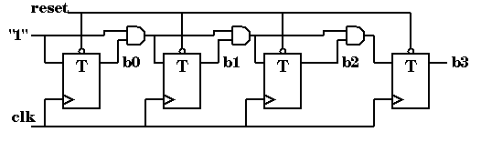
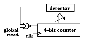
At the moment our design counts from 0 to 15 and then goes back to zero and continues counting. Figure 7 shows how the counter can be adapted to have a shorter cycle by using the reset signal. The mystery block is a simple piece of combinatorial logic which outputs a "1" when its input is a specific value. For instance, to create a counter which cycles from 0 to 11 (i.e. it cycles through 12 values), rather than 15, you design detection logic which raises a signal if the number 10 is detected (the cycle preceding the one where the action is to take place). Thus when the counter reaches 11, the reset line is active and so resets all of the dtypes on the next rising clock edge. Why is there a "global reset" signal included in the design?
EXERCISE 4: Design suitable combinatorial logic for the detector.
Let us now take a different example to illustrate a design style known as bit serial. In this technique, instead of having functions associated with each bit, a single functional block is used and the bits are cycled through that functional unit to produce the answer. Figure 8 shows a simple design to illustrate: a bit-serial addition. In this diagram two n-bit numbers are added together to make an (n+1)-bit sum. The 2 n-bit registers on the left are parallel-loaded shift-registers. The register on the right is simply a shift register. The unit between them is a 1-bit adder which consists of combinatorial logic to output the sum and carry of 3 input signals, a dtype to retains the value of the carry from the previous cycle and a final dtype to hold the sum output (see figure 9).
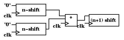
According to this definition, the shift register on the right is simply a series of dtypes where the output q of one is connected to the input d of the next. The other 2 registers are a similar arrangement using a module which we have designed previously (which?) adding the feature that if the control signal is raised, the signals on the parallel inputs will be clocked into the two registers. If that control signal is then lowered for subsequent cycles, the values will be shifted through the adder unit and the sum value is shifted into the output shift register, and (n+1) clock cycles later the operation is complete.
EXERCISE 5: Design the two types of shift register i.e. for both draw a schematic of one bit and show how this combines into a full shift register

Consider why it might be thought necessary to include a reset signal in the design of the dtype in the adder, and then discuss why it is not.
EXERCISE 6: Design the car/sum unit from boolean gates.
This may seem a very ponderous way to do a simple addition of 2 n-bit numbers, especially considering the overheads of the 3 shift registers. However, if a large number of arithmetic operations are to be performed, the arithmetic units may be connected directly to each other without intervening shift registers. Thus, the design requires parallel-loaded shift-registers at the inputs, and a shift register for the final result; and the intervening arithmetic operations are performed on a bit stream passing through the units. Figure 10 illustrates how the addition of 4 n-bit numbers can be achieved using only 3 one-bit adders.

EXERCISE 7: Using the counter from the previous example to generate the control signal for the parallel loaded shift register, construct a bit serial design which adds together 8 8-bit numbers every 12 clock cycles producing a sum which is held throughout the next 12 clock cycles. You will need to add a new type of register to hold the result.
Of course, addition can be done in a parallel fashion as shown in Figure 11. In this design, new values are clocked into registers A and B on every cycle and the sum of these values is clocked into register C on the following cycle.

EXERCISE 8: Using the combinatorial logic you designed in the serial implementation, show how the n-adder units are connected. How wide is register C? What becomes of the final carry from the adder units?
Notice that we have done the design of the bit
parallel implementation by constructing the logic for a single bit and then
replicating it n times. This is known as bit-slice.